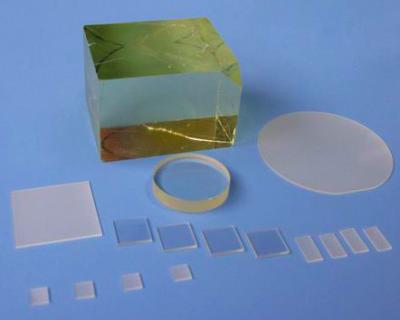
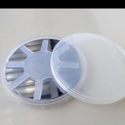
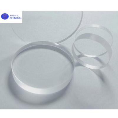
Het Wafeltje van het indiumfosfide
(33)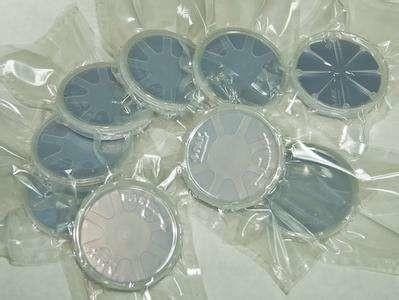
Het zwarte Wafeltje van het Indiumfosfide, Halfgeleiderwafeltje voor LD-Toepassing
Prijs: by case
MOQ: 5pcs
Tijd om te bezorgen: 1-4weeks
Merk: zmkj
Hoog licht:mgo substraat, Gap-wafeltje
de substraten van 2inch 3inch 4inch InP voor LD-toepassing, halfgeleiderwafeltje, InP-wafeltje, enig kristalwafeltje
InP introduceert
InP enig kristal
De tCZgroei (gewijzigde Czochralski-methode) wordt gebruikt om één enkel kristal door een booroxyde vloeibare encap... Bekijk meer
➤ Op bezoek komen Website
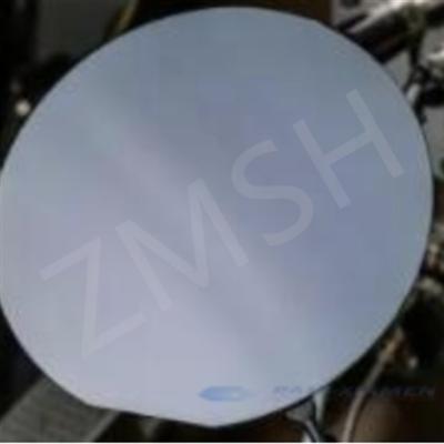
Van het de Platenindium van Duitsland Optisch van het het Fosfidewafeltje Uitstekend de Halfgeleidermateriaal
Prijs: by case
MOQ: 3pcs
Tijd om te bezorgen: 1-4weeks
Merk: zmkj
Hoog licht:mgo substraat, Gap-wafeltje
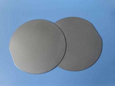
De Wafeltjes van germanium Enige Kristallen, de optische platen van Duitsland
Germaniumsubstraten
Toepassing: germaniumwafeltje in productie van halfgeleiderapparaat wordt gebruikt, infrarood straal optisch apparaat, dalend materiaal van zonnecel die.
Hoofdbezitstermijnen
... Bekijk meer
➤ Op bezoek komen Website
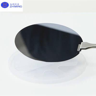
Van de de Lenshalfgeleider van Duitsland van het de Substrateninp Indium het Wafeltje van het het Galliumfosfide
Prijs: by case
MOQ: 3pcs
Tijd om te bezorgen: 1-4weeks
Merk: zmkj
Hoog licht:Van het de lensindium van Duitsland het Fosfidewafeltje, het Wafeltje van het het Indiumfosfide van halfgeleidersubstraten, inp het enige kristal van Duitsland
van het Germanium Enige Kristallen van 4inch 6inch de substratenwafeltjes van Duitsland, de aangepaste optische lens van Duitsland
Germaniumsubstraten
Toepassing: germaniumwafeltje in productie van halfgeleiderapparaat wordt gebruikt, infrarood straal optisch apparaat, dalend materiaal van zo... Bekijk meer
➤ Op bezoek komen Website
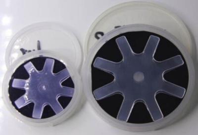
4 Wafeltje van het Fosfideinp van het duim Semi-Insulating Indium voor LD-Laserdiode
Prijs: by case
MOQ: 10pcs
Tijd om te bezorgen: 3-4weeks
Merk: zmkj
Hoog licht:inp wafeltje, mgo substraat
4inch Semi-Insulating Wafeltje van InP van het Indiumfosfide voor LD-Laserdiode, halfgeleiderwafeltje, het wafeltje van 3inch InP, enig kristalwafer2inch 3inch 4inch InP substraten voor LD-toepassing, halfgeleiderwafeltje, InP-wafeltje, enig kristalwafeltje
InP introduceert ... Bekijk meer
➤ Op bezoek komen Website
3.58 dichtheidsmgo Substraat/Mgo het Kristalsubstraat van het Wafeltjemagnesiumoxide
Prijs: by case
MOQ: 10pcs
Tijd om te bezorgen: 1-4weeks
Merk: zmkj
Hoog licht:inp wafeltje, Gap-wafeltje
MgO substraten, 10X10mm MgO wafeltje, halfgeleiderwafeltje, het kristalsubstraat van Magnesiumoxide(mgo), MgO van de kristallenleverancier WAFELTJE 5x5mmProductomschrijving:Het magnesiumoxide (MgO) is uitstekend want monocrystalline substraat wijd in productie van de ferroelectric dunne film wordt g... Bekijk meer
➤ Op bezoek komen Website
De Substraten van de de Wafeltjeshalfgeleider van Inp van germanium Enige Kristallen
Prijs: by case
MOQ: 3pcs
Tijd om te bezorgen: 1-4weeks
Merk: zmkj
Hoog licht:inp de substraten van de wafeltjeshalfgeleider, De wafeltjes van het halfgeleidergermanium inp, de substraten van germanium enige kristallen
van het Germanium Enige Kristallen van 4inch 6inch de substratenwafeltjes van Duitsland, de aangepaste optische lens van Duitsland
Germaniumsubstraten
Toepassing: germaniumwafeltje in productie van halfgeleiderapparaat wordt gebruikt, infrarood straal optisch apparaat, dalend materiaal van zo... Bekijk meer
➤ Op bezoek komen Website

Semi Isolerend 2 Duim 50mm n-Type het Proefwafeltje van het het Indiumfosfide van InP
Prijs: by case
MOQ: 3pcs
Tijd om te bezorgen: 3-4weeks
Merk: zmkj
Hoog licht:50mm het Wafeltje van het indiumfosfide, Het semi Isolerende Wafeltje van het indiumfosfide, n type inp wafeltje
van het n-type van 2inch dia50.8mm het proef eerste Wafeltje van het het indiumfosfide ranginp
4inch Semi-Insulating Wafeltje van InP van het Indiumfosfide voor LD-Laserdiode, halfgeleiderwafeltje, het wafeltje van 3inch InP, enig kristalwafer2inch 3inch 4inch InP substraten voor LD-toepassing, hal... Bekijk meer
➤ Op bezoek komen Website
Hoog Brekingsdsp-het Germaniumwafeltje van Oppervlaktege
Prijs: by case
MOQ: 3pcs
Tijd om te bezorgen: 1-4weeks
Merk: zmkj
Hoog licht:DSP-het Wafeltje van het Oppervlaktegermanium, hoog brekingsgermaniumwafeltje, DSP-het wafeltje van Oppervlakteduitsland
Type P van 2inch 4inch 6inch N het type smeerde de Wafeltjes van Germanium Enige Kristallen,
De optische platen van germanium Enige Kristallen
Het wafeltje van Duitsland/het venster van Duitsland
Het germanium (Duitsland) is het aangewezen lens en venstermateriaal voor systemen van de ho... Bekijk meer
➤ Op bezoek komen Website
Het Optische Inp Wafeltje van Duitsland, het Wafeltje van het het Indiumfosfide van het Halfgeleiderapparaat
Prijs: by case
MOQ: 3pcs
Tijd om te bezorgen: 1-4weeks
Merk: zmkj
Hoog licht:Optisch inpwafeltje van Duitsland, Wafeltje van het het Indiumfosfide van Duitsland het Optische, het wafeltje van het halfgeleiderapparaat inp
De Wafeltjes van germanium Enige Kristallen, de optische platen van Duitsland
Germaniumsubstraten
Toepassing: germaniumwafeltje in productie van halfgeleiderapparaat wordt gebruikt, infrarood straal optisch apparaat, dalend materiaal van zonnecel die.
Hoofdbezitstermijnen
P... Bekijk meer
➤ Op bezoek komen Website
De Groeikubus Crystal Mgo Substrates, Magnesiumoxidekristal van boogfrankrijk
Prijs: by case
MOQ: 10pcs
Tijd om te bezorgen: 1-4weeks
Merk: zmkj
Hoog licht:Mgo van boogfrankrijk substraten, Mgo van het kubuskristal substraten, mgo magnesiumoxidekristal
MgO substraten, 10X10mm MgO wafeltje, halfgeleiderwafeltje, het substraat van het Magnesiumoxide (MgO) kristal, MgO van de kristallenleverancier WAFELTJE 5x5mmProductomschrijving:Het magnesiumoxide (MgO) is uitstekend want monocrystalline substraat wijd in productie van de ferroelectric dunne film w... Bekijk meer
➤ Op bezoek komen Website

Van het het Indiumfosfide van germanium Enige Kristallen Optische Lens 4/6 Duim van Duitsland Wafeltje Aangepaste
Prijs: by case
MOQ: 3pcs
Tijd om te bezorgen: 1-4weeks
Merk: zmkj
Hoog licht:inp wafeltje, Gap-wafeltje
van het Germanium Enige Kristallen van 4inch 6inch de substratenwafeltjes van Duitsland, de aangepaste optische lens van Duitsland
Germaniumsubstraten
Toepassing: germaniumwafeltje in productie van halfgeleiderapparaat wordt gebruikt, infrarood straal optisch apparaat, dalend materiaal van ... Bekijk meer
➤ Op bezoek komen Website

N / P Type Germaniumwafeltje, de Platendiameter 0,5 ~ 150mm van de Germaniumoptica
Prijs: by case
MOQ: 3pcs
Tijd om te bezorgen: 1-4weeks
Merk: zmkj
Hoog licht:inp wafeltje, mgo substraat
type P van 2inch 4inch 6inch N het type smeerde de Wafeltjes van Germanium Enige Kristallen,
De optische platen van germanium Enige Kristallen
Het wafeltje van Duitsland/het venster van Duitsland
Het germanium (Ge) is het aangewezen lens en venstermateriaal voor systemen van de hoge p... Bekijk meer
➤ Op bezoek komen Website
De primaire/Proef van het het Fosfidewafeltje van het Rangindium Dikte 350um voor LD
Prijs: by case
MOQ: 3pcs
Tijd om te bezorgen: 1-4weeks
Merk: zmkj
Hoog licht:mgo substraat, Gap-wafeltje
2inch-van de n-Type p-Type van het de rangindium dikte350um primair rang Proef van het het Fosfidekristal de substratenwafeltje van InP voor LD
Is het het enige kristalmateriaal van het indiumfosfide één van belangrijkste halfgeleidersamenstelling, die zeer belangrijke grondstof voor laserdiod... Bekijk meer
➤ Op bezoek komen Website

Germanium Substraat GE Platte ramen Optische lenzen Thermische beeldvorming Toepassingen En Infrarood spectroscopie Hoge hardheid
Prijs: Negotiable
MOQ: Negotiable
Tijd om te bezorgen: 2-4 weeks
Merk: ZMSH
Hoog licht:Thermische beeldvorming Toepassingen Germaniumsubstraat, Infrarood spectroscopie Germaniumsubstraat, Substraat van germanium met een hoge hardheid
Productbeschrijving
Germaniumsubstraat GE Platte ramen Optische lenzen Thermische beeldvorming Toepassingen en infrarood spectroscopie Hoge hardheid
Germaniumvenster (Ge) is een chemisch inert materiaal met een toelaatbaar spectrumbereik van 2-12 μm, dat een veel gebruikt infraroodoptisch materiaal... Bekijk meer
➤ Op bezoek komen Website
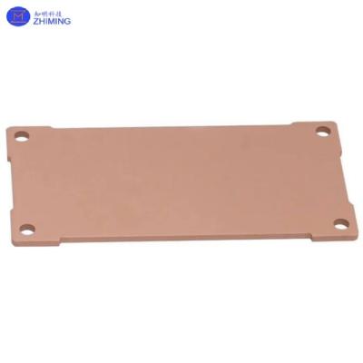
Koperen warmtebak Substraat platte bodem pin type hoogvermogen elektronisch apparaat Cu≥99.9%
Prijs: by case
MOQ: Negotiable
Tijd om te bezorgen: 2-4weeks
Merk: ZMSH
Hoog licht:Cu≥99, 9% Substraat voor warmteafvoeringen, hoogvermogen Heat Sink Substrate
Samenvatting van cbovenwarmteafzuigingssubstraat
Koperen warmtebak Substraat platte bodem pin type hoogvermogen elektronisch apparaat Cu≥99.9%
Koperwarmtebaksubstraat is een warmteafvoerend element gemaakt van puur koper (Cu≥99,9%) met een hoge thermische geleidbaarheid of een koperen le... Bekijk meer
➤ Op bezoek komen Website

InAs Indium Arsenide2inch 3inch 4inch Single Crystal Substrate N/P Type Halfronderaar Waferdikte 300-800um
Prijs: Negotiable
MOQ: Negotiable
Tijd om te bezorgen: 2-4 weeks
Merk: ZMSH
Hoog licht:4 inch Indium Arsenide Wafer, 3 inch Indium Arsenide Wafer, 2 inch Indium Arsenide Wafer
Productbeschrijving
InAs Indium Arsenide2inch 3inch 4inch Single Crystal Substrate N/P Type Halfronderaar Waferdikte 300-800um
Indium InAs of indium arsenide monolithisch is een halfgeleider samengesteld uit indium en arseen.Indiumarsenide wordt gebruikt voor het bouwen van infrarooddetectoren in h... Bekijk meer
➤ Op bezoek komen Website
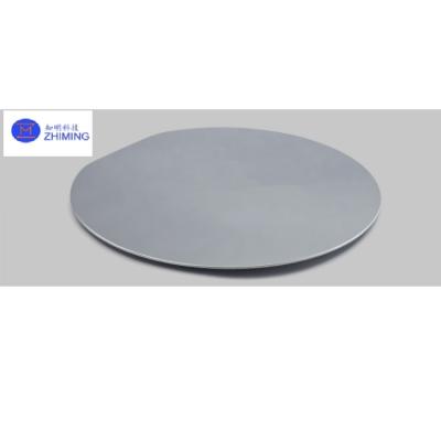
Ge-Germanium Wafer Halfgeleider Substraten <111> Concentrerende fotovoltaïsche CPV maatvormen
Prijs: Negotiable
MOQ: Negotiable
Tijd om te bezorgen: 2-4 weeks
Merk: ZMSH
Hoog licht:CPV-germaniumwafer, op maat gemaakte wafers van germanium, van de soort gebruikt voor de vervaardiging van elektrische motoren, met een vermogen van niet meer dan 50 W
Productbeschrijving
Ge germanium wafer halfgeleidersubstraten < 111> concentrerende fotovoltaïsche CPV maatvormen
Germanium heeft goede halfgeleider eigenschappen.en pentavalente elementenDe methode is gebaseerd op de methode van de methode van de methode van de methode van de methode.De Comm... Bekijk meer
➤ Op bezoek komen Website
Magnesiumoxide zuiverheid 95% MgO Filmsubstraat 5x5 10x10 20x20 Dikte 0,5 mm 1,0 mm Oriëntatie <001> <110> <111>
Prijs: by case
MOQ: 10pcs
Tijd om te bezorgen: 1-4weeks
Merk: zmkj
Hoog licht:5x5 MgO-filmsubstraat, 20 x 20 MgO-filmsubstraat, 10x10 MgO-filmsubstraat
Magnesiumoxide zuiverheid 95% MgO-filmsubstraat 5x5 10x10 20x20 dikte 0,5 mm 1,0 mm oriëntatie <001> <110> <111> Productbeschrijving:
Magnesiumoxide (MgO) enkelkristal van dunne film is een hoogwaardig substraatmateriaal met uitstekende fysische en chemische eigenschappen, zoals... Bekijk meer
➤ Op bezoek komen Website
InAs Wafer Doped Zn 2 Inch Indium Arsenide Wafer Dia 50mm Dikte 500um <100> Op maat
Prijs: Negotiable
MOQ: Negotiable
Tijd om te bezorgen: 2-4 weeks
Merk: ZMSH
Hoog licht:Gepersonaliseerde Indium Arsenide Wafer, 2 inch Indium Arsenide Wafer, 500um Indium Arsenide Wafer
2 inch Indium Arsenide Wafer InAs Epitaxiale Wafer voor LD Laser Diode, halfgeleider epitaxiale wafer, 3 inch InAs-Zn wafer,InAs-Zn-substraten voor LD-toepassingen, halfgeleiderwafer, Indium Arsenide Laser Epitaxial Wafer Kenmerken van InAs-Zn-wafer - gebruik maken van InAs-wafers voor de vervaardig... Bekijk meer
➤ Op bezoek komen Website
DFB wafer N-InP substraat epiwafer actieve laag InGaAlAs/InGaAsP 2 4 6 inch voor gassensor
Prijs: Negotiable
MOQ: Negotiable
Tijd om te bezorgen: 2-4weeks
Merk: ZMSH
Hoog licht:2 inch InP-substraat epiwafer, 4 inch InP substraat epiwafer, 6 inch InP substraat epiwafer
DFB wafer N-InP substraat epiwafer actieve laag InGaAlAs/InGaAsP 2 4 6 inch voor gassensor
DFB wafer N-InP substraat epiwafer's brief
Een Distributed Feedback (DFB) -wafer op een n-type Indiumfosfide (N-InP) -substraat is een kritisch materiaal dat wordt gebruikt bij de productie van hoogwaardi... Bekijk meer
➤ Op bezoek komen Website