Sic Epitaxial Wafeltje
(42)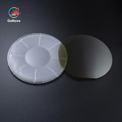
4 inch 4H-SiC Substraat P-niveau SI 500.0±25.0μm MPD≤5/cm2 Resistiviteit≥1E5Ω·cm Voor krachtige microgolf
Prijs: Negotiable
MOQ: Negotiable
Tijd om te bezorgen: 3-4 week days
Merk: GaNova
Hoog licht:4H-SiC-substraat van P-niveau, Microwave 4H-SiC-substraat, 4 inch 4H-SiC substraat
Van het het substraatniveau p van JDCD03-002-002 4inch 4H-sic Si 500.0±25.0μm MPD≤5/cm2 Resistivity≥1E5Ω·cm voor macht en microgolfapparaten
Overzicht
Sic wordt gebruikt voor de vervaardiging van apparaten zeer met hoog voltage en high-power zoals dioden, machtstransistors, en de apparate... Bekijk meer
Contact nu

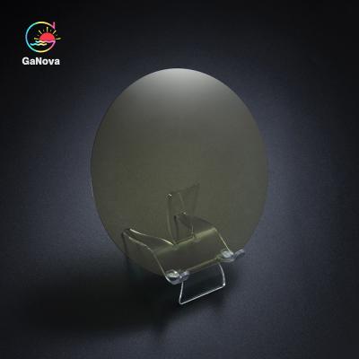
4 inch 4H-SiC Substraat P-Level SI 500.0±25.0μM MPD≤0.3/Cm2 Resistiviteit≥1E9Ω·Cm Voor krachtige magnetron
Prijs: Negotiable
MOQ: Negotiable
Tijd om te bezorgen: 3-4 week days
Merk: GaNova
Hoog licht:Microwave 4H-SiC-substraat, 4 inch 4H-SiC substraat, 4H-SiC-substraat P-niveau
JDCD03-002-001 4inch 4H-SiC substraat P-niveau SI 500.0±25.0μm MPD≤0.3/cm2 Weerstand≥1E9Ω·cm voor stroom- en microgolfapparaten
Overzicht
SiC heeft een hogere thermische geleidbaarheid dan GaAs of Si, wat betekent dat SiC-apparaten theoretisch kunnen werken met hogere vermogensdichtheden dan... Bekijk meer
Contact nu
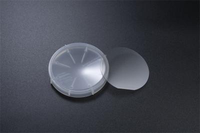
4 inch 4H-SiC-substraat P-niveau N-type 350,0 ± 25,0 μM MPD≤0,5/Cm2 Weerstand 0,015Ω•Cm—0,025Ω•Cm
Prijs: Negotiable
MOQ: Negotiable
Tijd om te bezorgen: 3-4 week days
Merk: GaNova
Hoog licht:4inch SiC Substrate
4inch 4H-SiC-substraat D-niveau N-type 350,0 ± 25,0 μm MPD≤5/cm2 Resistiviteit 0,015Ω•cm—0,025Ω•cm voor stroom- en microgolfapparaten
Overzicht
Apparaten op hoge temperatuur
Omdat SiC een hoge thermische geleidbaarheid heeft, verspreidt SiC warmte sneller dan andere halfgeleidermaterialen.H... Bekijk meer
Contact nu
2 inch Power Device High Electron Mobility Transistor Epitaxiale Wafer
Prijs: Negotiable
MOQ: 5
Tijd om te bezorgen: Negotiable
Merk: Ganova
Hoog licht:sic epitaxial wafer 2 Inch, Power Device sic epitaxial wafer, High Electron Mobility Transistor Epitaxial Wafer
Introduction to GaN on Silicon HEMT Epi wafer Silicon based gallium nitride HEMT epitaxial wafer is a high electron mobility transistor (HEMT) epitaxial wafer based on gallium nitride (GaN) material. Its structure mainly includes AlGaN barrier layer, GaN channel layer, AlN buffer layer, and silicon ... Bekijk meer
Contact nu
2 inch GaN op Silicon HEMT Epi wafer voor Power-apparaat
Prijs: Negotiable
MOQ: 5
Tijd om te bezorgen: Negotiable
Merk: Ganova
Hoog licht:GaN On Silicon HEMT Epi Wafer, 2 Inch Epi Wafer, Power Device Epi Wafer
Introduction to GaN on Silicon HEMT Epi wafer Silicon based gallium nitride HEMT epitaxial wafer is a high electron mobility transistor (HEMT) epitaxial wafer based on gallium nitride (GaN) material. Its structure mainly includes AlGaN barrier layer, GaN channel layer, AlN buffer layer, and silicon ... Bekijk meer
Contact nu
AlGaN-barrière 4 inch GaN op Silicon HEMT Epi wafer galliumnitride GaN-op-Si
Prijs: Negotiable
MOQ: 5
Tijd om te bezorgen: Negotiable
Merk: Ganova
Hoog licht:4 inch sic epitaxial wafer, 4 inch sic epi wafer, 4 inch sic epi wafers
Introduction to GaN on Silicon HEMT Epi wafer Silicon based gallium nitride HEMT epitaxial wafer is a high electron mobility transistor (HEMT) epitaxial wafer based on gallium nitride (GaN) material. Its structure mainly includes AlGaN barrier layer, GaN channel layer, AlN buffer layer, and silicon ... Bekijk meer
Contact nu
6 inch GaN op silicium HEMT Epi Wafer Power Device Gallium Nitride GaN op Si
Prijs: Negotiable
MOQ: 5
Tijd om te bezorgen: Negotiable
Merk: Ganova
Hoog licht:6 Inch sic epitaxial wafer, 6 Inch sic epi wafer, 6 Inch sic epi wafers
Introduction to GaN on Silicon HEMT Epi wafer Silicon based gallium nitride HEMT epitaxial wafer is a high electron mobility transistor (HEMT) epitaxial wafer based on gallium nitride (GaN) material. Its structure mainly includes AlGaN barrier layer, GaN channel layer, AlN buffer layer, and silicon ... Bekijk meer
Contact nu
GaN violette laser op silicium 2 inch GaN op silicium HEMT Epi wafer UV LD Epi wafer
Prijs: Negotiable
MOQ: 5
Tijd om te bezorgen: Negotiable
Merk: Ganova
Hoog licht:2 inch sic epitaxial wafer, 2 inch sic epi wafer, 2 inch sic epi wafers
Introduction to GaN on Silicon HEMT Epi wafer Silicon based gallium nitride HEMT epitaxial wafer is a high electron mobility transistor (HEMT) epitaxial wafer based on gallium nitride (GaN) material. Its structure mainly includes AlGaN barrier layer, GaN channel layer, AlN buffer layer, and silicon ... Bekijk meer
Contact nu
2 inch GaN op Silicon Blue LD Epi wafer GaN blauwe laser op silicium
Prijs: Negotiable
MOQ: 5
Tijd om te bezorgen: Negotiable
Merk: Ganova
Hoog licht:2 inch sic epitaxial wafer, 2 inch sic epi wafer, 2 inch sic epi wafers
Introduction to GaN on Silicon HEMT Epi wafer Silicon based gallium nitride HEMT epitaxial wafer is a high electron mobility transistor (HEMT) epitaxial wafer based on gallium nitride (GaN) material. Its structure mainly includes AlGaN barrier layer, GaN channel layer, AlN buffer layer, and silicon ... Bekijk meer
Contact nu
Blauwe LED GaN op Silicon Wafer Blauwe Laser GaN Epitaxiale Wafer
Prijs: Negotiable
MOQ: 5
Tijd om te bezorgen: Negotiable
Merk: Ganova
Hoog licht:Silicon Based Gallium Nitride Epitaxial Wafer, HEMT epitaxial wafer, 4 inch sic epitaxial wafer
Introduction to GaN on Silicon HEMT Epi wafer Silicon based gallium nitride HEMT epitaxial wafer is a high electron mobility transistor (HEMT) epitaxial wafer based on gallium nitride (GaN) material. Its structure mainly includes AlGaN barrier layer, GaN channel layer, AlN buffer layer, and silicon ... Bekijk meer
Contact nu
2 inch GaN op Silicon Green LED Epi wafer Gallium Nitride op Silicon
Prijs: Negotiable
MOQ: 5
Tijd om te bezorgen: Negotiable
Merk: Ganova
Hoog licht:2 inch sic epitaxial wafer, 2 inch sic epi wafer, 2 inch sic epi wafers
Introduction to GaN on Silicon Green LED Epi wafer GaN on Silicon Green LED Epi wafer are semiconductor structures formed on silicon substrate materials through epitaxial growth technology for manufacturing green light-emitting diodes (LEDs). It is a key intermediate material in the manufacturing of... Bekijk meer
Contact nu

4 inch GaN op Silicon Green LED Epi wafer SiC epitaxiale wafers
Prijs: 1000
MOQ: 5
Tijd om te bezorgen: Negotiable
Merk: Ganova
Hoog licht:4 inch sic epitaxial wafer, 4 inch sic epi wafer, 4 inch sic epi wafers
Introduction to GaN on Silicon Green LED Epi wafer GaN on Silicon Green LED Epi wafer are semiconductor structures formed on silicon substrate materials through epitaxial growth technology for manufacturing green light-emitting diodes (LEDs). It is a key intermediate material in the manufacturing of... Bekijk meer
Contact nu

4 inch uGaN op silicium ongedoopte galliumnitride op Silicon Epitaxial Wafer
Prijs: 1000
MOQ: 5
Tijd om te bezorgen: Negotiable
Merk: Ganova
Hoog licht:4 inch sic epitaxial wafer, 4 inch sic epi wafer, 4 inch sic epi wafers
Introduction to GaN on Silicon Green LED Epi wafer GaN on Silicon Green LED Epi wafer are semiconductor structures formed on silicon substrate materials through epitaxial growth technology for manufacturing green light-emitting diodes (LEDs). It is a key intermediate material in the manufacturing of... Bekijk meer
Contact nu

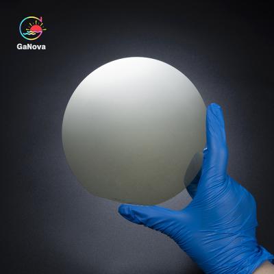
150.0mm +0mm/-0.2mm sic Epitaxial Wafeltje Geen Secundaire Vlakte 3mm
Prijs: Negotiable
MOQ: Negotiable
Tijd om te bezorgen: 3-4 week days
Merk: GaNova
Hoog licht:150.0 mm SiC Epitaxial Wafer, silicon carbide wafer 3mm, SiC Epitaxial Wafer No Secondary Flat
JDCD03-001-003 Overview SiC boules (crystals) are grown, machined into ingots, and then sliced into substrates, which are subsequently polished. A thin SiC epitaxial layer is then grown on top of this substrate to create an epi-wafer. Today, the semiconductor industry is expanding at a rapid rate, w... Bekijk meer
Contact nu
47,5 mm ± Epitaxial Wafeltje 150,0 mm +0mm/-0.2mm Parallelle to<11-20>±1° van 1,5 mm sic
Prijs: Negotiable
MOQ: Negotiable
Tijd om te bezorgen: 3-4 week days
Merk: GaNova
Hoog licht:446mm SiC Epitaxial Wafer, 4 H epitaxial silicon wafer, UKAS SiC Epitaxial Wafer
47.5 mm ± 1.5 mm SiC Epitaxial Wafer 150.0 mm +0mm/-0.2mm Parallel to±1° JDCD03-001-003 Overview Currently, there are two main types of SiC wafers. The first type is the polished wafer, which is a single silicon carbide disc. It is made of high-purity SiC crystals, and can be 100mm or 150mm in diame... Bekijk meer
Contact nu

4H sic Epitaxial Wafeltje ≤0.2 /cm2 0.015Ω•cm-0.025Ω•cm 150,0 mm +0mm/-0.2mm
Prijs: Negotiable
MOQ: Negotiable
Tijd om te bezorgen: 3-4 week days
Merk: GaNova
Hoog licht:4H SiC Epitaxial Wafer, silicon carbide wafer ISO9001, SiC Epitaxial Wafer 0.2 /Cm2
4H SiC Epitaxial Wafer ≤0.2 /Cm2 0.015Ω•Cm—0.025Ω•Cm 150.0 mm +0mm/-0.2mm JDCD03-001-004 Overview The 200-mm wafers can be used for a variety of applications. These wafers are 50% thinner than the standard silicon wafer, so the 200-mm diameter can be used for more SiC devices. The 200-mm size is muc... Bekijk meer
Contact nu

4H sic Epitaxial Wafeltje 0.015Ω•cm-0.025Ω•Cm ≤4000/cm ² 150,0 mm +0mm/-0.2mm
Prijs: Negotiable
MOQ: Negotiable
Tijd om te bezorgen: 3-4 week days
Merk: GaNova
Hoog licht:4H SiC Epitaxial Wafer, silicon epi wafer 0.025Ω•Cm, SiC Epitaxial Wafer 0.015Ω•Cm
4H SiC Epitaxial Wafer 0.015Ω•cm—0.025Ω•cm ≤4000/cm2 150.0 mm +0mm/-0.2mm JDCD03-001-003 Overview The next type is beta silicon carbide. Beta SiC is produced at temperatures higher than 1700 degrees Celsius. Alpha carbide is the most common, and has a hexagonal crystal structure similar to Wurtzite.... Bekijk meer
Contact nu

P-niveau 2 inch SiC-substraat voor stroomapparaten en microgolfapparaten
Prijs: Negotiable
MOQ: Negotiable
Tijd om te bezorgen: 3-4 week days
Merk: GaNova
Hoog licht:P Level SiC Substrate, Microwave Devices silicon carbide substrate, 2 Inch SiC Substrate
P-Level 4H-N/SI260um±25um 2-Inch SiC Substrate For Power Devices And Microwave Devices JDCD03-001-001 2-inch SiC substrate P-level 4H-N/SI260μm±25μm for power devices and microwave devices Overview Key features Optimizes targeted performance and total cost of ownership for next generation power elec... Bekijk meer
Contact nu

2 inch SiC-substraat 350 μm voor veeleisende vermogenselektronica
Prijs: Negotiable
MOQ: Negotiable
Tijd om te bezorgen: 3-4 week days
Merk: GaNova
Hoog licht:2 Inch SiC Substrate, Demanding Power Electronics 2 inch wafer, SiC Substrate 350um
P-Level 2-Inch SiC Substrate 4H-N/SI260μm±25μm For Demanding Power Electronics JDCD03-001-001 2-inch SiC substrate P-level 4H-N/SI260μm±25μm for power devices and microwave devices Overview High crystal quality for demanding power electronics As transportation, energy and industrial markets evolve, ... Bekijk meer
Contact nu