GaAs Epi-wafel
(15)
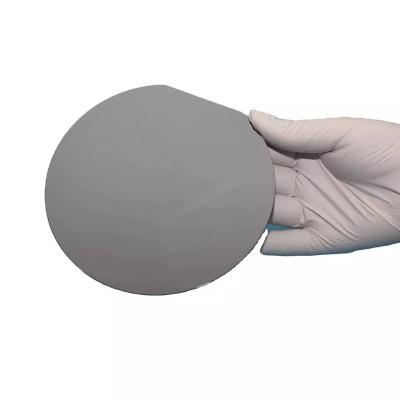
18mm GaAs Si Wafer 2inch GaAs Undoped Substrates VGF S-C-N
Prijs: Negotiable
MOQ: Negotiable
Tijd om te bezorgen: 3-4 week days
Merk: GaNova
Hoog licht:18mm GaAs Si Wafer, GaAs Undoped Substrates VGF, GaAs Si Wafer 2inch
2inch GaAs (100) Undoped Substrates Overview GaAs is often used as a substrate material for the epitaxial growth of other III-V semiconductors, including indium gallium arsenide, aluminum gallium arsenide and others. Gallium arsenide (chemical formula GaAs) is a semiconductor compound used in some d... Bekijk meer
➤ Op bezoek komen Website

2inch GaAs Undoped Substrates GaAs Epi Wafer 0.4E18 To 1E18
Prijs: Negotiable
MOQ: Negotiable
Tijd om te bezorgen: 3-4 week days
Merk: GaNova
Hoog licht:Undoped GaAs Epi Wafer, gaas substrates 1E18, GaAs Epi Wafer 0.4E18
2inch GaAs (100) Undoped Substrates GaAs-Si Wafer 0.4E18~1E18 Overview The RF devices produced with GaAs substrates are commonly used in wireless communication applications, including wireless networks (WLAN), mobile communication, 4G/5G base stations, satellite communications, and WiFi communicatio... Bekijk meer
➤ Op bezoek komen Website

JDCD10-001-001 2 inch GaAs (100) ongedoteerde substraten
Prijs: Negotiable
MOQ: Negotiable
Tijd om te bezorgen: 3-4 week days
Merk: GaNova
2inch GaAs (100) Undoped Substrates Overview Gallium arsenide of a GaAs Wafer has the attribute of generating laser light from electricity in a direct manner. There are two types of GaAs Wafer; polycrystalline and single crystal. These wafers are utilized in micro electronics and opto electronics pr... Bekijk meer
➤ Op bezoek komen Website

Optische communicatie Galliumarsenide Substraat LED's
Prijs: Negotiable
MOQ: Negotiable
Tijd om te bezorgen: 3-4 week days
Merk: GaNova
Hoog licht:Optical gallium arsenide substrate, Optical Communications Epi Wafer, LEDs gallium arsenide substrate
2inch GaAs (100) Undoped Substrates Overview Gallium arsenide is used in the manufacture of light-emitting diode s (LEDs), which are found in optical communications and control systems. Gallium arsenide can replace silicon in the manufacture of linear ICs and digital ICs. Linear (also called analog ... Bekijk meer
➤ Op bezoek komen Website

JDCD10-001-002 2 inch GaAs (100) Si-gedoteerde substraten
Prijs: Negotiable
MOQ: Negotiable
Tijd om te bezorgen: 3-4 week days
Merk: GaNova
2inch GaAs (100) Si-doped substrates Overview GaAs is often used as a substrate material for the epitaxial growth of other III-V semiconductors, including indium gallium arsenide, aluminum gallium arsenide and others. Gallium arsenide of a GaAs Wafer has the attribute of generating laser light from ... Bekijk meer
➤ Op bezoek komen Website

JDCD10-001-005 2inch GaAs(111) Zn-gedoteerde substraten
Prijs: Negotiable
MOQ: Negotiable
Tijd om te bezorgen: 3-4 week days
Merk: GaNova
2inch GaAs(111) Zn-doped substrates Overview GaAs crystals can be created through three different methods. One of the more common methods is the vertical gradient freeze process, which involves growing crystals and slicing them, followed by edge rounding and polishing them into wafers. Another metho... Bekijk meer
➤ Op bezoek komen Website

JDCD10-001-003 2inch GaAs(100) Zn-gedoteerde substraten
Prijs: Negotiable
MOQ: Negotiable
Tijd om te bezorgen: 3-4 week days
Merk: GaNova
2inch GaAs(100) Zn-doped substrates Overview Gallium arsenide of a GaAs Wafer has the attribute of generating laser light from electricity in a direct manner. There are two types of GaAs Wafer; polycrystalline and single crystal. These wafers are utilized in micro electronics and opto electronics pr... Bekijk meer
➤ Op bezoek komen Website

JDCD10-001-004 2inch GaAs (111) Si-Doped Substrates
Prijs: Negotiable
MOQ: Negotiable
Tijd om te bezorgen: 3-4 week days
Merk: GaNova
2inch GaAs (111) Si-doped substrates Overview Gallium in a GaAs Wafer is in general used in the production of semiconductors, barometers, light emitting diodes, thermometers and electronic circuits. It is a silvery metal and quite soft which makes it easy to be used in chips as well. Gallium element... Bekijk meer
➤ Op bezoek komen Website

VGF 2inch GaAs Epi Wafer Undoped Substraten Side Polished Etched
Prijs: Negotiable
MOQ: Negotiable
Tijd om te bezorgen: 3-4 week days
Merk: GaNova
Hoog licht:VGF GaAs Epi Wafer, gaas wafer thickness 350um, GaAs Epi Wafer Side Polished
2inch GaAs (100) Undoped Substrates Overview Gallium arsenide of a GaAs Wafer has the attribute of generating laser light from electricity in a direct manner. There are two types of GaAs Wafer; polycrystalline and single crystal. These wafers are utilized in micro electronics and opto electronics pr... Bekijk meer
➤ Op bezoek komen Website

51mm 2inch GaAs Wafer Undoped Substraten 7mm IF Lengte
Prijs: Negotiable
MOQ: Negotiable
Tijd om te bezorgen: 3-4 week days
Merk: GaNova
Hoog licht:2inch gaas wafer, gallium arsenide substrate 7mm, 51mm gaas wafer
50.8±0.2mm 2inch GaAs (100) Undoped Substrates 7±1mm IF Length Overview With the development of mini-LED and micro-LED, red light LEDs produced with GaAs substrates are increasingly used for display screens and in AR/VR. The conversion efficiency of a high-efficiency solar-cell panel based on GaAs i... Bekijk meer
➤ Op bezoek komen Website

VGF GaAs Undoped Substrates 2inch GaAs Si Dopant
Prijs: Negotiable
MOQ: Negotiable
Tijd om te bezorgen: 3-4 week days
Merk: GaNova
Hoog licht:VGF Undoped Substrates, GaAs substrates S-C-N, GaAs Undoped Substrates
2inch GaAs (100) Undoped Substrates (100)15°±0.5° Off TowardA 2inch GaAs (100) Undoped Substrates Overview GaAs is a semi-conductor material with excellent performance characteristics including direct band gap, high electron mobility, high-frequency low noise, and high conversion efficiency. GaAs-Si... Bekijk meer
➤ Op bezoek komen Website

17mm 2inch GaAs Epi Wafer Undoped Substrates 50.8mm
Prijs: Negotiable
MOQ: Negotiable
Tijd om te bezorgen: 3-4 week days
Merk: GaNova
Hoog licht:17mm GaAs Epi Wafer, epitaxial wafer 50.8mm, GaAs Epi Wafer 50.8mm
17±1mm OF Length 2inch GaAs (100) Undoped Substrates 50.8±0.2mm Overview The conversion efficiency of a high-efficiency solar-cell panel based on GaAs is up to 40%. At present, such solar-cell panels are widely used in unmanned aerial vehicle and solar auto applications. GaAs applications cover a la... Bekijk meer
➤ Op bezoek komen Website

S-C-N Conduct 2inch GaAs ongedoteerde substraten Hoge elektronenmobiliteit
Prijs: Negotiable
MOQ: Negotiable
Tijd om te bezorgen: 3-4 week days
Merk: GaNova
Hoog licht:S-C-N semiconductor substrate, GaAs-Si Wafer ISO, semiconductor substrate 17mm
S-C-N Conduct 2inch GaAs (100) Undoped Substrates High Electron Mobility Overview With the development of mini-LED and micro-LED, red light LEDs produced with GaAs substrates are increasingly used for display screens and in AR/VR. GaAs is a semi-conductor material with excellent performance characte... Bekijk meer
➤ Op bezoek komen Website

Halfgeleiderverbinding 2 inch GaAs Epi Wafer GaAs Si Wafer UKAS
Prijs: Negotiable
MOQ: Negotiable
Tijd om te bezorgen: 3-4 week days
Merk: GaNova
Hoog licht:GaAs Epi Wafer UKAS, 2inch GaAs Si Wafer, Semiconductor Gallium arsenide Wafer
GaAs-Si Wafer 2inch GaAs (100) Undoped Substrates (100)15°±0.5° Off TowardA Overview Gallium arsenide (chemical formula GaAs) is a semiconductor compound used in some diode s, field-effect transistor s (FETs), and integrated circuit s (ICs). The charge carriers, which are mostly electron s,move at h... Bekijk meer
➤ Op bezoek komen Website
2inch GaAs Epi Wafer GaAs Undoped Substraten VGF
Prijs: Negotiable
MOQ: Negotiable
Tijd om te bezorgen: 3-4 week days
Merk: GaNova
Hoog licht:GaAs Epi Wafer Undoped Substrates, GaAs-Si Wafer 2inch, 2inch GaAs Epi Wafer
GaAs-Si Wafer 2inch GaAs (100) Undoped Substrates EJ[0-1-1]±0.5° Overview GaAs applications cover a large variety of transistors for industry spanning optical fiber communication, wireless networks (WLAN), mobile handsets, blue tooth communications, satellite communications, monolithic microwave int... Bekijk meer
➤ Op bezoek komen Website