Fe Gesmeerd GaN Substrates Resistivity > 10 ⁶ Ω·De Apparaten van cm rf
Prijs: Negotiable
MOQ: Negotiable
Tijd om te bezorgen: 3-4 week days
Merk: GaNova
Hoog licht:ISO GaN Substrates, gan semiconductor wafer, Fe Doped GaN Substrates
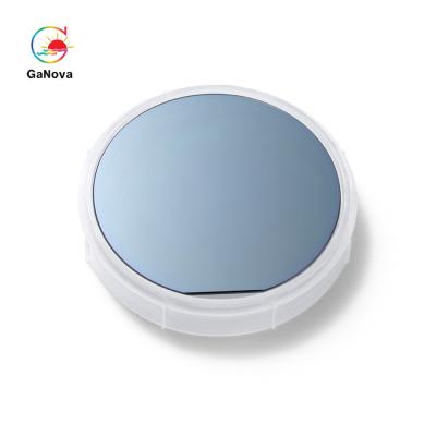
2inch C-face Fe-doped SI-type free-standing GaN single crystal substrate Resistivity > 106 Ω·cm RF devices The achieved breakdown voltage of the Fe-doped GaN epitaxial layer can be as high as 2457 V, which is attributed to the Fe-doped GaN epitaxial layer with higher resistance, which can sustain... Bekijk meer
➤ Op bezoek komen Website
2 inch Power Device High Electron Mobility Transistor Epitaxiale Wafer
Prijs: Negotiable
MOQ: 5
Tijd om te bezorgen: Negotiable
Merk: Ganova
Hoog licht:sic epitaxial wafer 2 Inch, Power Device sic epitaxial wafer, High Electron Mobility Transistor Epitaxial Wafer
Introduction to GaN on Silicon HEMT Epi wafer Silicon based gallium nitride HEMT epitaxial wafer is a high electron mobility transistor (HEMT) epitaxial wafer based on gallium nitride (GaN) material. Its structure mainly includes AlGaN barrier layer, GaN channel layer, AlN buffer layer, and silicon ... Bekijk meer
➤ Op bezoek komen Website
GaAs Epi-wafel
(15)
18mm GaAs Si Wafer 2inch GaAs Undoped Substrates VGF S-C-N
Prijs: Negotiable
MOQ: Negotiable
Tijd om te bezorgen: 3-4 week days
Merk: GaNova
Hoog licht:18mm GaAs Si Wafer, GaAs Undoped Substrates VGF, GaAs Si Wafer 2inch
2inch GaAs (100) Undoped Substrates Overview GaAs is often used as a substrate material for the epitaxial growth of other III-V semiconductors, including indium gallium arsenide, aluminum gallium arsenide and others. Gallium arsenide (chemical formula GaAs) is a semiconductor compound used in some d... Bekijk meer
➤ Op bezoek komen Website

XRD
Prijs: Negotiable
MOQ: Negotiable
Tijd om te bezorgen: 3-4 week days
Merk: GaNova
Hoog licht:Electronic Grade Single Crystal Diamond, Electronic Diamond Substrates, Heat Sink Single Crystal Diamond
XRD Bekijk meer
➤ Op bezoek komen Website

Verhoog de productie Rapid Thermal Processing RTP-SA-8 Annealing System
Prijs: Negotiable
MOQ: Negotiable
Tijd om te bezorgen: 3 month
Merk: Ganova
Hoog licht:Boost Production Rapid Thermal Processing, Rapid Thermal Processing Annealing System
1.Basic configuration of equipment system 1.1outline The Rapid Thermal Processing is a vertical semi-automatic 8-inch wafer rapid annealing furnace, which uses two layers of infrared halogen lamps as heat sources for heating. The internal quartz cavity is insulated and insulated, and the outer shell... Bekijk meer
➤ Op bezoek komen Website
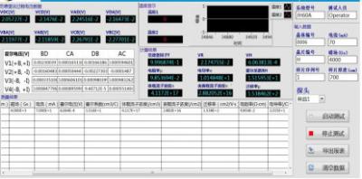
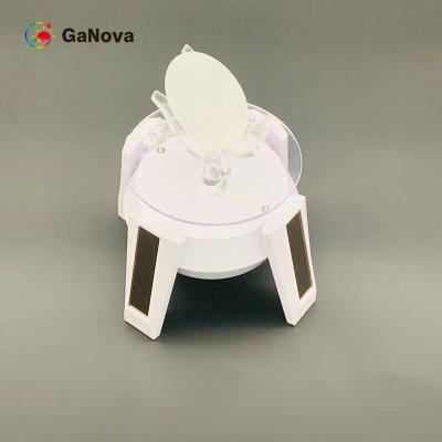
Hall Coefficient Hall Effect Sensor Tester Mobility Resistivity Measurement
Prijs: Negotiable
MOQ: 1
Tijd om te bezorgen: 8-10week days
Merk: GaNova
Hoog licht:Hall Effect Sensor Tester Mobility Resistivity, carrier concentration hall effect instrument, Hall Effect Sensor Tester semiconductor
Hall Coefficient Hall Effect Sensor Tester mobility resistivity measurement Product Overview: Hall effect tester is used to measure the carrier concentration, mobility, resistivity, Hall coefficient and other important parameters, and these parameters of semiconductor materials to understand the ele... Bekijk meer
➤ Op bezoek komen Website
ALN 10*10mm2 AlN enkelkristal 400±50μM S/P/R-klasse
Prijs: Negotiable
MOQ: 1
Tijd om te bezorgen: Negotiable
Merk: GaNova
Hoog licht:ALN aluminum nitride wafer, 2H aluminum nitride wafer, 10*10mm2 aln wafer
AlN substrate is one of the most popular ceramic substrate which has excellent heat resistance, high mechnical strength , abrasion resistance and small dielectric loss . The surface of AlN substrate is quite smooth and low porosity . Aluminium Nitride has higher thermal conductivity , compared to al... Bekijk meer
➤ Op bezoek komen Website

94um Laser Diode Chip Slope Efficiency 1.0W/A Wavelength 915nm
Prijs: Negotiable
MOQ: Negotiable
Tijd om te bezorgen: Negotiable
Merk: GaNova
Hoog licht:94um Laser Diode Chip, high power laser diode chip, 1.0W/A Laser Diode Chip
94μm Laser Diode Chip Slope Efficiency 1.0W/A Wavelength 915nm 915nm 10W COS Diode Laser Chip On Submount Design For low power consumption it is essential that the output from the laser diode (LD) is efficiently coupled to the optical waveguide, and there are several approaches reported in the liter... Bekijk meer
➤ Op bezoek komen Website

100.0mm Silicon Carbide Crystal 4" P Grade Politype 4H
Prijs: Negotiable
MOQ: Negotiable
Tijd om te bezorgen: 3-4 week days
Hoog licht:Silicon Carbide Crystal P Grade, single crystal silicon carbide, Silicon Carbide Crystal 4H
100.0mm±0.5mm SiC Seed Crystal 4" P Grade 4.0°±0.2° Politype 4H SiC Seed Crystal 4" PGrade SiC can withstand a voltage gradient (or electric field) over eight times greater than than Si or GaAs without undergoing avalanche breakdown. This high breakdown electric field enables the fabricati... Bekijk meer
➤ Op bezoek komen Website
Ga2O3 Wafeltje
(13)
Sn Doping Ga2O3 Wafer Single Crystal Substraat 10x10mm2
Prijs: Negotiable
MOQ: Negotiable
Tijd om te bezorgen: 3-4 week days
Merk: GaNova
Hoog licht:Sn Doping Ga2O3 Wafer, 0.8mm Gallium Oxide wafer, Ga2O3 Wafer 10x10mm2
10x10mm2 (-201) Fe-doped free-standing Ga2O3 single crystal substrate Product grade single polishing Thickness 0.6~0.8mm FWHM<350arcsec,Ra≤0.3 nm Optoelectronic devices, insulating layers of semiconductor materials, and UV filters Among these different phases of Ga2O3, the orthorhombic β-gallia stru... Bekijk meer
➤ Op bezoek komen Website
siliciumwafeltje
(26)
JDCD07-001-001 4-inch SOI epitaxiaal wafeltje voor MEMS-verwerking
Prijs: Negotiable
MOQ: 1
Tijd om te bezorgen: 3-4 week days
Merk: GaNova
4-Inch SOI Epitaxial Wafer For MEMS Processing Overview Although silicon crystals may look metallic, they are not entirely metals. Due to the "free electrons" that move easily between atoms, metals are good conductors of electricity, and electricity is the movement of electrons. A pure sil... Bekijk meer
➤ Op bezoek komen Website
Sapphire Wafer
(19)
Het c-Vliegtuig Sapphire Substrate Wafer van JDCD08-001-006 6inch
Prijs: Negotiable
MOQ: Negotiable
Tijd om te bezorgen: Negotiable
JDCD08-001-006 6inch C-Plane Sapphire Substrate Wafer Sapphires are Second Only to Diamonds in Durability Diamond is the most durable naturally occurring element on earth and ranks as a 10 out of 10 on Mohs Scale of Mineral Hardness. Sapphires are also very durable and rank as a 9 out of 10 on Mohs ... Bekijk meer
➤ Op bezoek komen Website

UKAS Patterned Sapphire Substrates Flat Edge Angle
Prijs: Negotiable
MOQ: 1
Tijd om te bezorgen: Negotiable
Merk: GaNova
Hoog licht:UKAS Patterned Sapphire Substrates, al2o3 substrate 430um, Patterned Sapphire Substrates OEM
50.80±0.10mm Patterned Sapphire Substrates Flat Edge Angle A-Plane±0.2o 2inch Patterned Sapphire Substrates,LED Chip,Substrate Material The efficacy enhancement of GaN-based LEDs with the patterned-sapphire substrate technique is generally attributed to the improvement in both light extraction effic... Bekijk meer
➤ Op bezoek komen Website

6 inch Wafer Houder Schoonmaken van bloemenmanden en handvatten
Prijs: Negotiable
MOQ: 1
Tijd om te bezorgen: Negotiable
Hoog licht:6inch Wafer Holder, wafer cassette carrier, 25 PCS Wafer Holder
6inch Wafer Holder Cleaning Flower Baskets And Handles PFA Cassette / Cassette of wafer can be customized and designed by customers’ request, able to resist strong acid, strong hydrofluoric acid, strong base and heat up to 200~220℃, use to deliver wafers in acid & base process of Fabrication f... Bekijk meer
➤ Op bezoek komen Website

0.1mm/s To 600mm/s Wafer Dicing Machine X Axis Cutting Range 260mm
Prijs: Negotiable
MOQ: 1
Tijd om te bezorgen: 8-10week days
Merk: GaNova
Hoog licht:0.1mm/s Wafer Dicing Machine, wafer saw machine 260mm, 600mm/s Wafer Dicing Machine
DAD3350 Wafer Dicing Machine 0.1 ~ 600mm/s X-Axis Cutting Range 260mm Improved throughput The DAD3350 achieves improvement in throughput by increasing the speed of each axis. Ease of use Operability is improved with installation of an LCD touch screen and Graphical User Interface (GUI). Easy operati... Bekijk meer
➤ Op bezoek komen Website